MCS-170 Project 7: Logic Circuits - Part
II
Due: In Class
Project Task
In this lab, you will use a logic circuit simulator to investigate
the design and analysis of logic circuits that carry out addition of
binary digits. During the lab you
will be asked a series of questions.
Record your answers and turn them in to the instructor at the end of
the lab period.
In Lab
In the first part of this lab we investigated simple gates such as AND,
OR, NOT, and XOR gates. We saw how these gates could be combined to
form more complex logical circuits. One of the exercises from Part I
was to investigate a half-adder.
This is a circuit that adds two binary digits, A and B, and has two
outputs, which represent the sum digit of A+B and the carry digit.
Review the diagram on page 294 of the text to refresh your memory on
the design of a half-adder.
We will again use the logic simulator located at
http://www.gac.edu/~hvidsten/courses/MC170/simcir121/simcir.html
Open a new browser window and start the simulator befor proceeding on
with this lab.
EXERCISE 1:
At the bottom of the list of gates on the left side of the
simulator you will see a gate labeled "Half Adder". Drag this gate into
the window, hook up two switches labeled "A"and "B", hook up LED's to
these switches and to the outputs, and test out the half-adder. Write
down the logic table for the half-adder as follows, and verify that it
works just the same as the half-adder circuit you built from scratch in
Part I.
A
B | SUM CARRY
-----+------------
0 0 |
0 1 |
1 0 |
1
1 |
The term "half-adder" is used to refer to this circuit because it only
partially solves the problem of adding two multiple-digit numbers. When you
add two numbers, you not only sum up the digits in a particular column,
but you also have to keep track of whether there is a carry digit
coming from adding up a previous column.
For example, consider the following addition of A=1011 and B=111:
c c c c
1 0 1 1
+ 1 1 1
---------
1 0 0 1 0
When adding the digits in the second, third, and fourth columns, we
have a carry of 1 coming in from the column to the right. A
better adder circuit would have a third input, labeled "cin" that would
keep track of this carry from a previous column. To construct
such a "full" adder circuit, we'll need three inputs and two
outputs. The inputs will be the two numbers A and B, and also the carry
digit coming in from a previous column. The outputs will be the digit
for the sum and a carry digit. Since we'll have both an input carry and
an output carry, we'll
designate them as "Cin" and "Cout". We'll use "Sum" to designate the
digit of the sum. How can we build a full-adder?
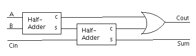
We can implement the full adder by using two
half-adder circuits. The first will add A and B to produce a partial
sum and a partial carry,
while the second will add Cin to the partial sum to produce the final
Sum output. If either half-adder produces a carry, there will be an
output
carry. Thus, Cout will be an OR function of the half-adder carry
outputs. The resulting full adder circuit is shown below.
EXERCISE 2:
Construct this circuit in the simulator using two half-adders
and an OR gate. Fill in the truth table for this circuit.
A
B Cin | Cout Sum
---------+-----------
0 0 0 |
0 0 1 |
0 1 0 |
0 1 1 |
1 0 0 |
1 0 1 |
1 1 0 |
1 1 1 |
EXERCISE 3:
We could build multiple copies of the previous circuit and use them to
build more complex circuits. This would be tedious. Fortunately, the
Circuit Simulator has built-in Full-Adder gates (the last gate in the
list of gates in the left-hand window). Read the discussion on
page 295 on how to connect full-adders together to add 4-digit numbers.
Then, use 4 full-adder circuits as shown on page 295 to construct a
4-bit adder circuit in your simulator. Test it out on different numbers
to verify that it is working. Then, hand in a printout of your circuit
(or have the instructor okay your circuit).
So far we have focused solely on arithmetic and logical operations of
the computer (activities of the ALU). How does memory get implemented
with logical gates? The simplest circuit for storing a 1-0 value is
called a
flip-flop.
This circuit is illustrated in Figures 16.17 and 16.18 of the text
(page 296).
EXERCISE 4: To build
this circuit in the simulator, use two "PushOn" switches for the two
inputs. These switches are normally off (0) and turn on (1) only when
pressed. Construct the flip-flop circuit in the simulator and then test
what happens when you press the "Set" and "Reset" buttons. Note
the "feed-back" wire that runs from the output of the circuit back to
the input of the lower AND gate. What purpose does this wire serve in
the circuit? Why is it reasonable to call this circuit a
flip-flop circuit? What feature makes it useful for storing (i.e., remembering) values?
Note that while recent labs have just been check-off labs, this
last question will be graded. Please answer it thoughtfully.
Project Report:
Hand in your answers to the exercises above.
Back to
MCS
170
home page